5 min read
Atomic Layer Processing Coating Techniques Enable Missions to See Further into the Ultraviolet Astrophysics observations at ultraviolet (UV) wavelengths often probe the most dynamic aspects of the universe. However, the high energy of ultraviolet photons means that their interaction with the materials that make up an observing instrument are less efficient, resulting in low overall throughput. New approaches in the development of thin film coatings are addressing this shortcoming by engineering the coatings of instrument structures at the atomic scale.
Researchers at the NASA Jet Propulsion Laboratory (JPL) are employing atomic layer deposition (ALD) and atomic layer etching (ALE) to enable new coating technologies for instruments measuring ultraviolet light. Conventional optical coatings largely rely on physical vapor deposition (PVD) methods like evaporation, where the coating layer is formed by vaporizing the source material and then condensing it onto the intended substrate. In contrast, ALD and ALE rely on a cyclic series of self-limiting chemical reactions that result in the deposition (or removal) of material one atomic layer at a time. This self-limiting characteristic results in a coating or etchings that are conformal over arbitrary shapes with precisely controlled layer thickness determined by the number of ALD or ALE cycles performed.
The ALD and ALE techniques are common in the semiconductor industry where they are used to fabricate high-performance transistors. Their use as an optical coating method is less common, particularly at ultraviolet wavelengths where the choice of optical coating material is largely restricted to metal fluorides instead of more common metal oxides, due to the larger optical band energy of fluoride materials, which minimizes absorption losses in the coatings. Using an approach based on co-reaction with hydrogen fluoride, the team at JPL has developed a variety of fluoride-based ALD and ALE processes.
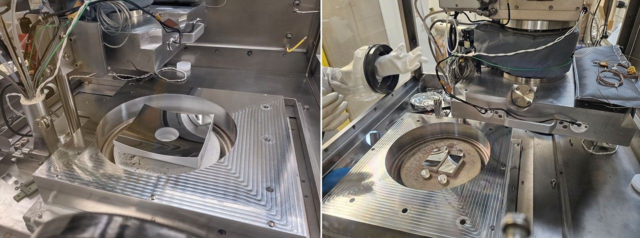
 (left) The Supernova remnants and Proxies for ReIonization Testbed Experiment (SPRITE) CubeSat primary mirror inside the ALD coating facility at JPL, the mirror is 18 cm on the long and is the largest optic coated in this chamber to-date. (right) Flight optic coating inside JPL ALD chamber for Pioneers Aspera Mission. Like SPRITE, the Aspera coating combines a lithium fluoride process developed at NASA GSFC with thin ALD encapsulation of magnesium fluoride at JPL. Image Credit: NASA-JPL In addition to these metal-fluoride materials, layers of aluminum are often used to construct structures like reflective mirrors and bandpass filters for instruments operating in the UV. Although aluminum has high intrinsic UV reflectance, it also readily forms a surface oxide that strongly absorbs UV light. The role of the metal fluoride coating is then to protect the aluminum surface from oxidation while maintaining enough transparency to create a mirror with high reflectance.
The use of ALD in this context has initially been pursued in the development of telescope optics for two SmallSat astrophysics missions that will operate in the UV: the Supernova remnants and Proxies for ReIonization Testbed Experiment (SPRITE) CubeSat mission led by Brian Fleming at the University of Colorado Boulder, and the Aspera mission led by Carlos Vargas at the University of Arizona. The mirrors for SPRITE and Aspera have reflective coatings that utilize aluminum protected by lithium fluoride using a novel PVD processes developed at NASA Goddard Space Flight Center, and an additional very thin top coating of magnesium fluoride deposited via ALD.
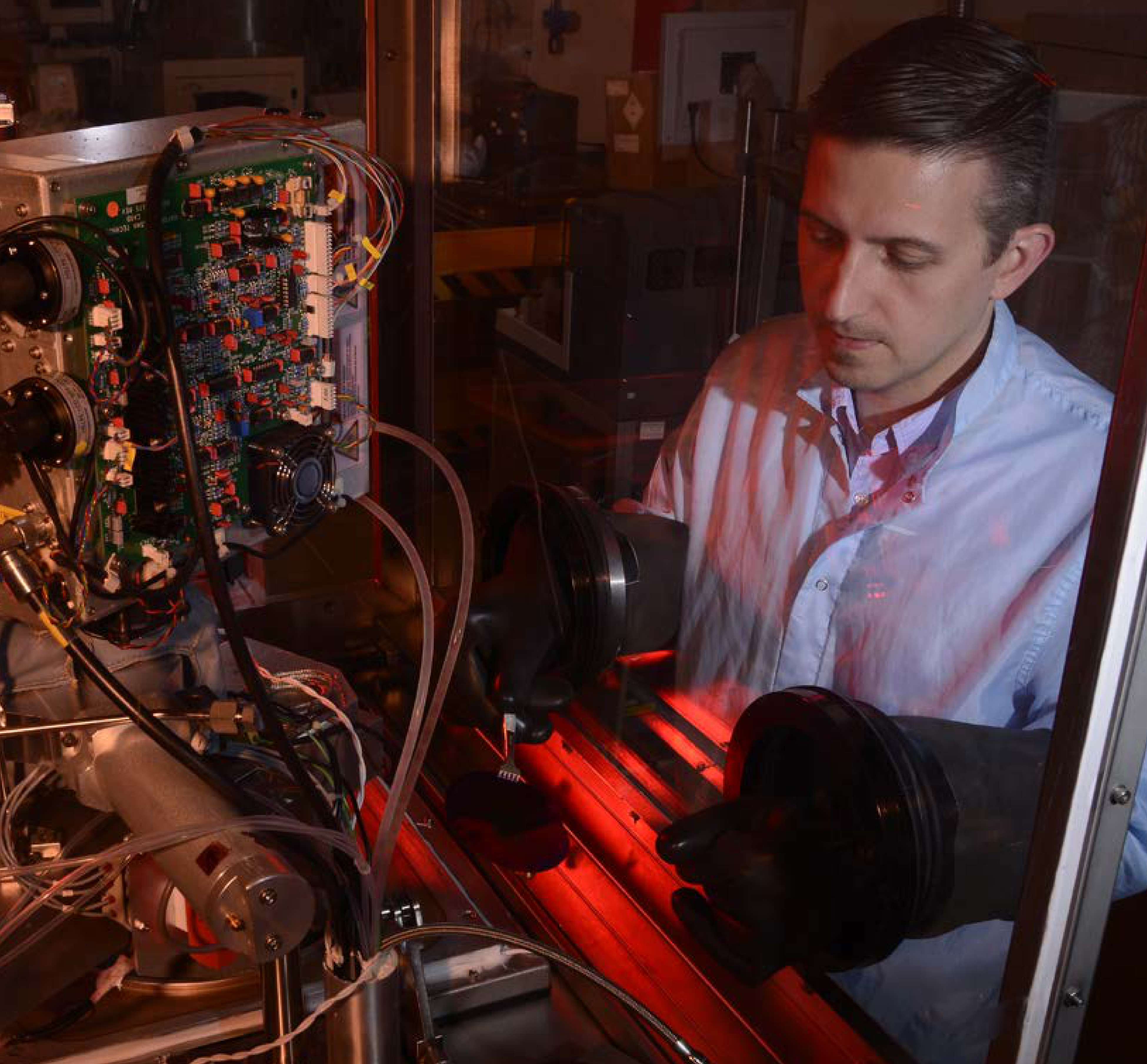
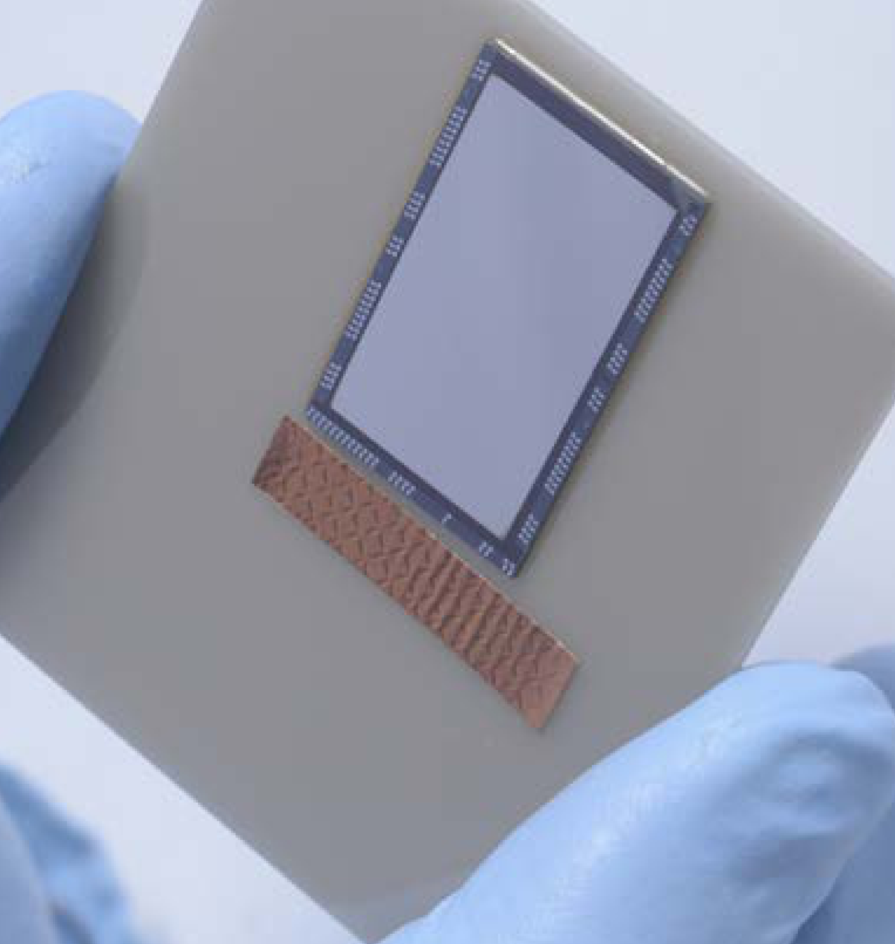
Multilayer structures of aluminum and metal fluorides can also function as bandpass filters (filters that allow only signals within a selected range of wavelengths to pass through to be recorded) in the UV. Here, ALD is an attractive option due to the inherent repeatability and precise thickness control of the process. There is currently no suitable ALD process to deposit aluminum, and so additional work by the JPL team has explored the development of a custom vacuum coating chamber that combines the PVD aluminum and ALD fluoride processes described above. This system has been used to develop UV bandpass filters that can be deposited directly onto imaging sensors like silicon (Si) CCDs. These coatings can enable such sensors to operate with high UV efficiency, but low sensitivity to longer wavelength visible photons that would otherwise add background noise to the UV observations.
Structures composed of multilayer aluminum and metal fluoride coatings have recently been delivered as part of a UV camera to the Star-Planet Activity Research CubeSat (SPARCS) mission led by Evgenya Shkolnik at Arizona State University. The JPL-developed camera incorporates a delta-doped Si CCD with the ALD/PVD filter coating on the far ultraviolet channel, yielding a sensor with high efficiency in a band centered near 160 nm with low response to out-of-band light.
For additional details, see the entry for this project on NASA TechPort
Project Lead: Dr. John Hennessy, Jet Propulsion Laboratory (JPL)
Details Last Updated Mar 18, 2025 Related Terms Technology Highlights Astrophysics Astrophysics Division Jet Propulsion Laboratory Science-enabling Technology


 5 min read NASA’s Webb Images Young, Giant Exoplanets, Detects Carbon Dioxide
 2 min read Hubble Sees a Spiral and a Star
 4 min read Discovery Alert: ‘Super-Earth’ Swings from Super-Heated to Super-Chill
